 Go to JKU Homepage

Dipl.-Ing. Dr. Patrick Hölzl
Dipl.-Ing. Dr. Patrick Hölzl is winner of the Prof. Werner Rieder-Preis 2019. He received the award from the association Verein zur Förderung der Schalterforschung for his PhD work “Detection of defective bond wire connections in integrated circuits utilizing a GMR line array developed for magnetic field measurements with high spatial resolution”. The award endowed with € 2.500,— was handed over at the evening event of the OVE Energietechnik Tagung on 16th October 2019 in the Messe Innsbruck.
Link to the article, opens an external URL in a new window

Supervisory committee: | |
|---|---|
Final exam: | |
Univ.-Prof. Dipl.-Ing. Dr. Bernhard Zagar Ao.Univ.-Prof. Dipl.-Ing. Dr.techn. Christian Magele, opens an external URL in a new window | September 10th, 2018 |
Supervisory committee: | Univ.-Prof. Dipl.-Ing. Dr. Bernhard Zagar Ao.Univ.-Prof. Dipl.-Ing. Dr.techn. Christian Magele, opens an external URL in a new window |
Final exam: | September 10th, 2018 |
Modern power electronic components must be able to operate with voltages and currents in the range of several kV and kA. In this context, the electrical interconnection between the semiconductor chip and its output pins, which is often realized by bond wires, is a crucial factor. To guarantee the current carrying capacity of the interconnections, redundant bond wires are typically implemented. However, due to this redundancy conventional electrical tests are not able to detect individual missing or insufficiently connected bond wires, since the impact on electrical parameters is usually diminishing. The semiconductor manufacturer Infineon initiated therefore the present PhD thesis, to develop a measurement method to detect such bonding faults. The developed method determines the current flowing within each bond wire based on the magnetic field distribution measured above the component. If one or more bond wires are missing, not only the current flow within the remaining wires increases, but also the resulting field distribution changes.
To evaluate the developed measurement method, the MOSFET switch BTS5120-2EKA from Infineon was selected. The BTS5120-2EKA possesses two independently switchable N-channel DMOSFETs, with each channel connected via three parallel bond wires to the output pins. An X-ray image of the chip is shown in Fig 1. Infineon also provided a series of test chips similar to the BTS5120-2EKA, where one or two bond wires in a single channel were missing.
Based on milling layer pictures of a BTS5120-2EKA a simplified geometric model of all current carrying bond wires was designed, consisting of six straight line conductor segments per wire, see Fig. 2. Utilizing the straight line conductor model and the law of biot-savart it was possible to calculate the magnetic field distribution above the component analytically. The results obtained from these calculations were essential for the design process of a magnetic sensor line array, consisting of 26 GMR sensor elements. A microscopic image of the GMR sensor line array is shown in Fig. 3.
After the production of the GMR sensor line array by Infineon, the GMR sensor elements were characterized in terms of sensitivity, non-linearity, temperature dependency, noise characteristic and spatial resolution. With the GMR sensor line array the field distributions above 400 samples, 100 BTS5120-2EKA and 300 test chips with different fault permutations of the bond wires were measured. Based on the measured data an inverse problem for determining the current flow within the bond wires was formulated. The solution of the inverse problem was derived by two different approaches, a model--based and a data-based one. The measurement results and determined current values for two different chip types are shown in Fig. 4. Using a threshold value method for the determined current flow values, it was possible to detect up to 99.33% of all fault permutation test chips without a misclassification of a single faultless BTS5120-2EKA.
Keywords: non--destructive testing, integrated circuits, bond wires, magnetic field sensors, GMR line array, inverse field problem
Datum: 6th April 2018
 Figure1: X-ray image of a BTS5120-2EKA with highlighted current paths of the two integrated N-channel DMOSFETs. For each channel three copper bond wires (denoted by {B1, B2, B3} and {B4, B5, B6}) establish the electrical interconnection between the semiconductor chip and its output pins OUT0/OUT1.
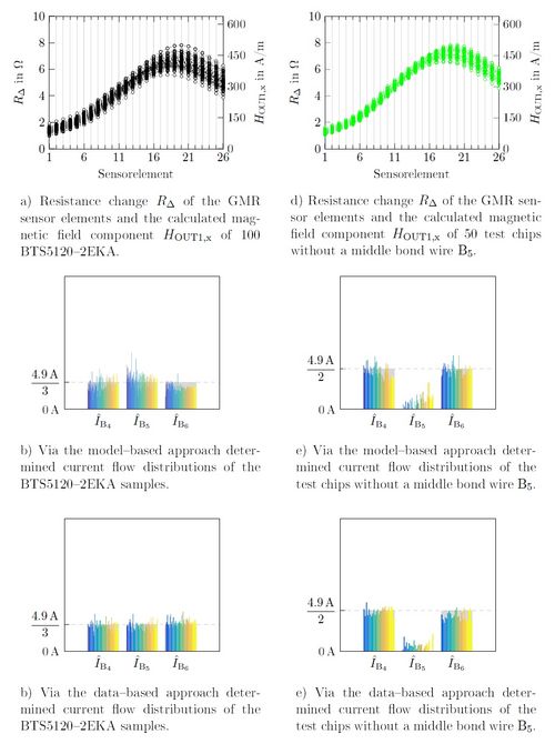 Figure 2: 3D-model of the current carrying bond wires and simplified geometric model, were each wire is approximated by six straight line conductor segments with vertices P0-P6.
 Figure 3: Microscopic image of the magnetic sensor line array integrated on a semiconductor chip and consisting of 26 GMR sensor elements.
 Figure 4: Results of the magnetic field measurements and the determination of the current flow distributions for two different chip types. For the measurements a current of 4.9A was applied to channel 1, with the bond wires {B4, B5, B6}. The determined current distributions on the right side are clearly indicating the absence of the middle bond wire B5 in the test chips.