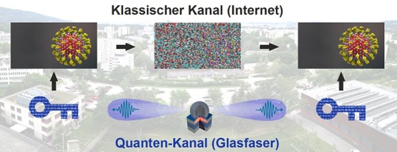
Research at the Institute of Semiconductor and Solid State Physics focuses on the growth, nanofabrication, characterization, modification and applications of semiconducting heterostructures and nanostructures of ferromagnetic structures and materials, oligomers, polymers and metals. Our focus covers all aspects of nanostructures, ranging from fundamental investigations and modeling of physical properties to the realizing novel nanostructures in support of quantum optics, infrared optoelectronics, magnetic, spintronic and thermoelectric devices.
Nanostructures are fabricated using advanced lithography and processing techniques, including electron beam lithography, holographic lithography, as well as self-assembled growth of quantum dots and wires using molecular beam epitaxy, metal-organic vapor phase epitaxy and chemical synthesis. In this regard, the institute operates a Class-100 cleanroom facility containing all of the required processing equipment. The objective of nanofabrication is to produce defect-free structures in the sub-50-nm range with precise control of shapes and compositions, sharp heterointerfaces and excellent optical, electronic and magnetic properties. We focus particularly on developing site-control techniques to support the positioning of self-assembled nanostructures.
Institute of Semiconductor and Solid State Physics
Head of Institute
Adress
Johannes Kepler University of Linz
Altenberger Straße 69
4040 Linz
Location
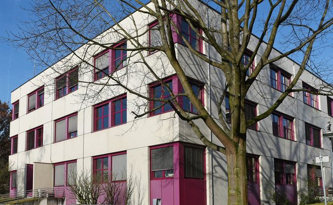
Semiconductor Physics building
Office hours
Mo-Fr: 09.00 - 15.00
Telephone
+43 732 2468-9600, -9639
Semiconductor Physics Division
Solid State Physics Division
News & Events
The Lise Meitner Lecture: Lisa Kaltenegger
Presentation by Lisa Kaltenegger: "Alien Earths: Searching for a Second Earth - Challenges, Opportunities and Adventures"


"Physics World 2020 Breakthrough of the Year"
Group Stangl involved in discovery of light emission of Si based material, (Nature 580, 205-209/2020)
See also article in Frankfurter Allgemeine Zeitung, 8 March 2021
 Go to JKU Homepage


